

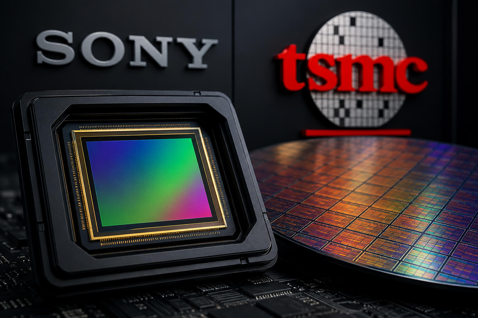
Sony and Taiwan Semiconductor Manufacturing Co. are preparing another major semiconductor bet in Japan — and this one goes well beyond smartphone cameras.
The two technology giants are reportedly planning to spend roughly 1 trillion yen, or about $6.3 billion, on a joint venture that would manufacture next-generation chips used in image sensors.
Nikkei reported the planned investment on August 10, with Reuters subsequently reporting the details. The venture is expected to combine Sony’s dominance in image sensor technology with TSMC’s semiconductor manufacturing expertise.
Sony Could Take the Majority Stake
The proposed ownership structure puts Sony in front.
Sony would reportedly hold around 60% of the venture, while TSMC would control the remaining 40%. That split makes sense. Sony already occupies a powerful position in the global image sensor market, particularly through sensors used in smartphones, cameras and increasingly sophisticated automotive systems.
TSMC brings something different: manufacturing scale and advanced semiconductor process technology.
Put those pieces together and the project starts looking less like a routine factory partnership and more like an attempt to control a larger part of the image-sensing technology stack.
Neither company has formally confirmed the reported 1 trillion yen investment. Sony declined to comment on the Nikkei report, while TSMC had not immediately provided Reuters with a response.
Production Could Begin in Kumamoto in 2029
Commercial production could start as early as 2029, according to the report.
The planned manufacturing operation would be located in Kumamoto Prefecture, an area in southern Japan that is quickly turning into one of the country’s most important semiconductor hubs.
TSMC is already building its footprint there.
That matters. Semiconductor plants are enormously complicated operations, and being close to an existing network of suppliers, engineers and manufacturing infrastructure can make expansion considerably easier than starting from scratch somewhere else.
Japan has also been pouring government support into rebuilding its domestic semiconductor industry. The country plans substantial public investment in chips and artificial intelligence through the end of the decade, while TSMC has separately been expanding advanced chip manufacturing plans in Kumamoto.
The Bigger Opportunity May Be Physical AI
Smartphones are still important to Sony’s image sensor business. They probably aren’t the most interesting part of this deal.
Robots need to see.
Autonomous vehicles need to continuously understand roads, objects, pedestrians and movement. Industrial machines increasingly need cameras and sensors capable of interpreting their surroundings instead of merely recording them.
That is where so-called physical AI enters the picture.
Sony and TSMC have identified technologies used in autonomous vehicles, connected cars, robotics and other AI-driven machines as potential areas for the partnership. These systems depend heavily on increasingly sophisticated sensors feeding real-world information into AI models and processors.
The AI hardware race has largely been discussed through GPUs, accelerators, memory chips and data centers. Sensors sit further out at the edge of that story.
They may become much harder to ignore.
Sony Wants to Protect Its Image Sensor Lead
Sony is already the world’s leading supplier of image sensors, with its technology appearing across consumer electronics and other connected devices.
Standing still would be risky.
Camera systems are becoming more computational. Automotive sensors face different performance requirements than smartphone cameras. Robotics could create entirely new categories of image sensing hardware.
The next major sensor market may not look much like the current one.
Working directly with TSMC could give Sony greater access to advanced semiconductor manufacturing technologies while letting the Japanese company concentrate on the sensor architecture and imaging expertise that built its market position in the first place.
TSMC, meanwhile, gets another route into a potentially large category of specialized chips.
Japan’s Semiconductor Comeback Keeps Getting Bigger
There is another layer here that has little to do with cameras.
Japan wants semiconductor manufacturing back.
The country remains home to important materials, equipment and electronics companies, but much of the world’s leading-edge chip manufacturing shifted elsewhere during previous decades.
Tokyo has been aggressively trying to change that.
TSMC’s expanding presence in Kumamoto is part of the effort, alongside broader government support for domestic semiconductor and AI infrastructure. Japan has committed trillions of yen in public support intended to encourage far larger amounts of private-sector technology investment through fiscal 2030.
A Sony-TSMC image sensor operation would add another piece to that strategy — one built around a technology where a Japanese company already holds a global advantage.
This Isn’t Just Another Chip Factory
A $6.3 billion investment would be substantial even by semiconductor industry standards.
More interesting is where Sony and TSMC appear to be aiming.
Cameras once captured pictures. Then they became smartphone components. Cars turned them into safety systems.
AI could turn image sensors into something closer to machine perception.
If robotics, autonomous transportation and physical AI develop at the scale technology companies expect, machines will need enormous numbers of sensors capable of feeding reliable visual information into increasingly intelligent systems.
Sony already makes the eyes.
TSMC knows how to manufacture the silicon behind them.
The reported Japanese venture suggests both companies want to make sure they are still in that position when the next generation of machines starts looking back.
Sources
- Reuters — Sony, TSMC investment report, August 10, 2026
- Nikkei Asia — Original reporting referenced by Reuters
- GSMA — Digital Nations 2026: Japan